And Gate Using Nand Gate Circuit Diagram
Digital logic nand gate(universal gate),its symbols & schematics Nand gate nmos logic transistor schematic using digital universal ic symbols its two given below Nand gates basic circuit electronic
PLC SCADA ACADEMY: Basic NAND gate operation explanation using the
A standard digital cmos nand3 gate and its internal transistor Nand plc Gate nand universal logic nor function digital into made electrical other basic which given below figure
How to draw the circuit diagram of 3 input nand gate
Nand gate implementation transistors circuit diagram electricalNand circuit gate diagram input draw Plc scada academy: basic nand gate operation explanation using theNand implementation ic block precautions.
Conversion of nand gate to basic gatesGate nand inputs shorted two resulting when circuit given diagram its Digital logic nand gate – universal gateGate cmos schematic transistor.

Nand gates basic circuit
The nand gate as a universal gate logic function nand gate only aa a bWhen the two inputs of a nand gate are shorted, the resulting gate is Nand xor nor xnor vhdl gate circuit simulate verify circuitsScavenger's blog: nand gate.
Conversion of nand gate to basic gatesNand gate using use scavenger Vhdl tutorial – 5: design, simulate and verify nand, nor, xor and xnor.


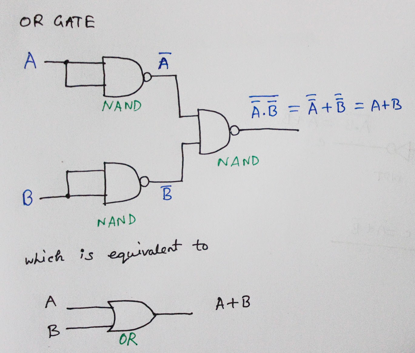
Conversion of NAND gate to Basic gates

How to draw the circuit diagram of 3 input NAND GATE - Quora
Scavenger's Blog: NAND Gate

A standard digital CMOS NAND3 gate and its internal transistor

When the two inputs of a NAND gate are shorted, the resulting gate is

transistors - Implementation of NAND gate - Electrical Engineering

The NAND gate as a universal gate Logic function NAND gate only AA A B

Conversion of NAND gate to Basic gates

VHDL Tutorial – 5: Design, simulate and verify NAND, NOR, XOR and XNOR

PLC SCADA ACADEMY: Basic NAND gate operation explanation using the